Clock Gating Check
Clock gating check是一种常见的时序检查,当gating signal控制clock signal时,其跳变必须满足时序要求以得到想要的gated clock。最常见的gating check发生在ICG cell上。ICG是常见的low power解决方案,通过在clock tree上插入ICG cell,来减少ICG后面clock buffer/register的不必要跳变,从而起到降低功耗的目的。其实,只要是多输入逻辑cell,只要满足两个条件,都需要做gating check。
1.clock gating check 的必要条件
clock gating check必须满足两个条件:
- clock pin上必须是有效clock signal。
- gating pin上必须是无效clock signal。
这里的有效clock signal是博主为了方便理解生造出来的。有效clock signal并不是仅仅说这个clock pin上有clock attribute,而且它的fanout必须至少满足以下之一:
- 有register的clock pin;
- 有output port;
- 有以clock pin所属clock的generated clock的sink.
与之对应,gating pin必须是data signal或者不满足上面三个条件的clock signal。
只有满足了clock pin和gating pin都满足要求,才会对这个logic cell做gating check。
SDC里,我们用set_clock_gating_check往往不能完全覆盖所有需要gating check的logic cell,这时工具会根据上文的gating check必要条件来推断需要gating check的点。
2.两种clock gating check
以与门和或门为代表,有两种类型的gating check:
- active-high clock gating check: gating signal为1时,clock signal可以穿过logic cell。比如AND/NAND cell。
- active-low clock gating check: gating signal为0时,clock signal可以穿过logic cell。比如OR/NOR cell。
3.case example
为了验证clock gating check,需要写一个简单的test module,verilog 如下:
1
2
3
4
5
6
7
8
9
10
11
12
13
module test ( A, CLK, OUT);
input A;
input CLK;
output OUT;

DFQD2BWP7T40P140HVT reg0 (.D(A), .CP(CLK), .Q(reg0out));
AN2D2BWP7T40P140HVT and1 (.A1(CLK), .A2(reg0out), .Z(and1out));
AN2D2BWP7T40P140HVT and2 (.A1(CLK), .A2(reg0out), .Z(and2out));
AN2D2BWP7T40P140HVT and3 (.A1(CLK), .A2(reg0out), .Z(OUT));
DFQD2BWP7T40P140HVT reg1 (.D(and1out), .CP(A), .Q());
DFQD2BWP7T40P140HVT reg2 (.D(A), .CP(and2out), .Q());

endmodule
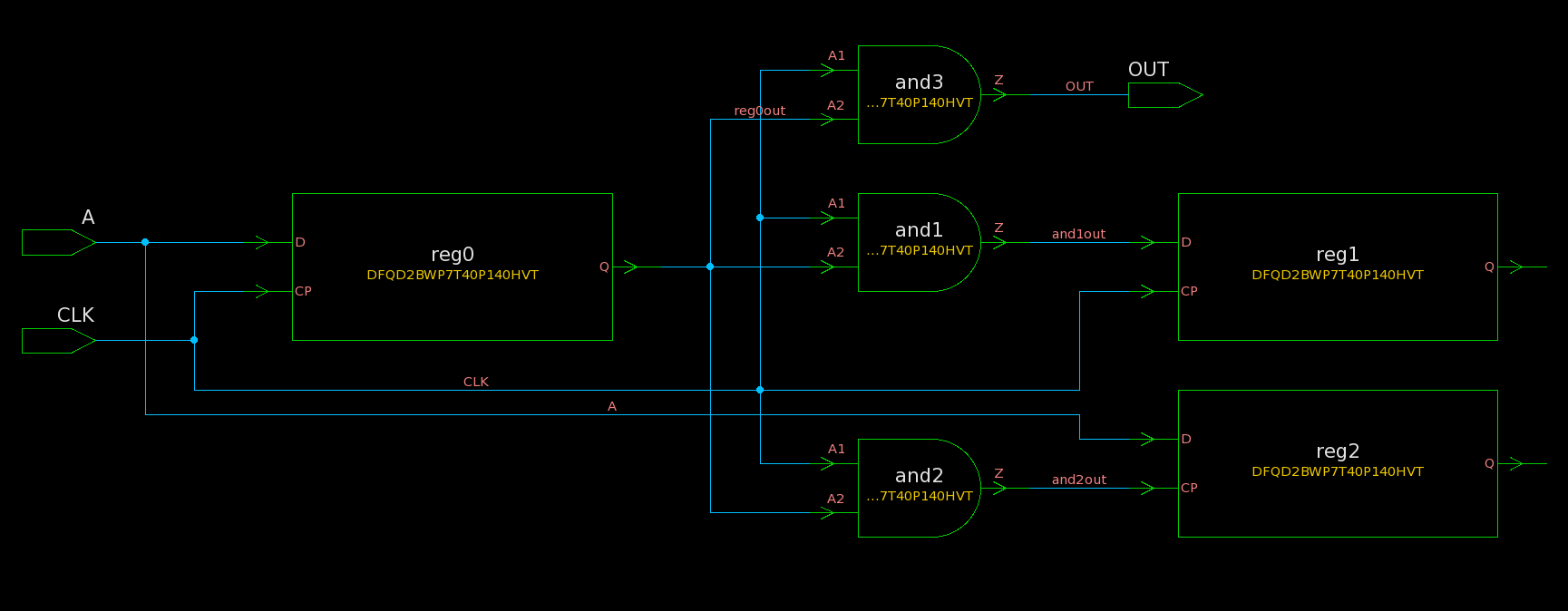
电路图如下:
 在port CLK处定义clock myclk,然后report timing :
1
2
3
4
5
6
7
8
9
10
11
12
13
14
15
16
17
18
19
20
21
22
23
24
25
26
27
28
29
30
31
32
33
34
35
36
37
38
39
40
41
42
43
44
45
46
47
48
49
50
51
52
53
54
55
56
57
58
59
60
61
62
63
64
65
66
67
68
69
70
71
72
73
74
75
76
77
78
79
80
81
82
83
84
85
86
87
88
89
90
91
92
93
94
95
96
97
98
pt_shell> create_clock -name myclk -period 2 [get_ports CLK]
1
pt_shell> report_timing -to and1/A2 -group **clock_gating_default**
****************************************
Report : timing
        -path_type full
        -delay_type max
        -max_paths 1
        -group **clock_gating_default**
        -sort_by slack
Design : test
Version: I-2013.12
Date   : Fri Oct  6 17:43:59 2017
****************************************

Warning: There is 1 invalid end point for constrained paths. (UITE-416)
Warning: There is 1 invalid end point for unconstrained paths. (UITE-416)
No Paths.

1
pt_shell> report_timing -to and2/A2 -group **clock_gating_default**
****************************************
Report : timing
        -path_type full
        -delay_type max
        -max_paths 1
        -group **clock_gating_default**
        -sort_by slack
Design : test
Version: I-2013.12
Date   : Fri Oct  6 17:43:15 2017
****************************************


  Startpoint: reg0 (rising edge-triggered flip-flop clocked by myclk)
  Endpoint: and2 (rising clock gating-check end-point clocked by myclk)
  Path Group: **clock_gating_default**
  Path Type: max

  Point                                    Incr       Path
  ---------------------------------------------------------------
  clock myclk (rise edge)                  0.00       0.00
  clock network delay (ideal)              0.00       0.00
  reg0/CP (DFQD2BWP7T40P140HVT)            0.00       0.00 r
  reg0/Q (DFQD2BWP7T40P140HVT)             0.13       0.13 f
  and2/A2 (AN2D2BWP7T40P140HVT)            0.00       0.13 f
  data arrival time                                   0.13

  clock myclk (rise edge)                  2.00       2.00
  clock network delay (ideal)              0.00       2.00
  clock reconvergence pessimism            0.00       2.00
  and2/A1 (AN2D2BWP7T40P140HVT)                       2.00 r
  clock gating setup time                  0.00       2.00
  data required time                                  2.00
  ---------------------------------------------------------------
  data required time                                  2.00
  data arrival time                                  -0.13
  ---------------------------------------------------------------
  slack (MET)                                         1.87


1
pt_shell> report_timing -to and3/A2 -group **clock_gating_default**
****************************************
Report : timing
        -path_type full
        -delay_type max
        -max_paths 1
        -group **clock_gating_default**
        -sort_by slack
Design : test
Version: I-2013.12
Date   : Fri Oct  6 17:43:32 2017
****************************************

  Point                                    Incr       Path
  ---------------------------------------------------------------
  clock myclk (rise edge)                  0.00       0.00
  clock network delay (ideal)              0.00       0.00
  reg0/CP (DFQD2BWP7T40P140HVT)            0.00       0.00 r
  reg0/Q (DFQD2BWP7T40P140HVT)             0.13       0.13 f
  and3/A2 (AN2D2BWP7T40P140HVT)            0.00       0.13 f
  data arrival time                                   0.13

  clock myclk (rise edge)                  2.00       2.00
  clock network delay (ideal)              0.00       2.00
  clock reconvergence pessimism            0.00       2.00
  and3/A1 (AN2D2BWP7T40P140HVT)                       2.00 r
  clock gating setup time                  0.00       2.00
  data required time                                  2.00
  ---------------------------------------------------------------
  data required time                                  2.00
  data arrival time                                  -0.13
  ---------------------------------------------------------------
  slack (MET)                                         1.87


1
对于这三个与门,都是A1 pin为clock pin, A2 pin位gating pin。
and2/A1的fanout有reg2/CP,为myclk的sink,所以and2/A1是有效clock signal, and1需要clock gating check;
and3/A1的fanout有output port OUT,所以and3/A1也是有效clock singal, and3需要clock gating check;
and1/A1的fanout既没有clock sink,也没有output port,所以and1不需要clock gating check.
如果在and2后面定义clock呢?
1
2
3
4
5
6
7
8
9
10
11
12
13
14
15
16
17
18
19
20
21
22
23
24
25
26
27
28
29
30
31
32
33
34
35
36
37
38
39
pt_shell> create_clock -name myclk2 -period 2 and2/Z
Warning: Creating a clock on internal pin 'and2/Z'. (UITE-130)
1
pt_shell> report_timing -to and2/A2 -group **clock_gating_default**
Warning: No clock-gating check was inferred for clock myclk at pins and2/A2 and and2/A1 of cell and2 because no clock pins could be found in the fanout for the propagating clock. (PTE-101)
Information: Abandoning fast timing updates. (PTE-018)
Information: Inferring 1 clock-gating checks. (PTE-017)
****************************************
Report : timing
        -path_type full
        -delay_type max
        -max_paths 1
        -group **clock_gating_default**
        -sort_by slack
Design : test
Version: I-2013.12
Date   : Fri Oct  6 18:12:49 2017
****************************************

Warning: There is 1 invalid end point for constrained paths. (UITE-416)
Warning: There is 1 invalid end point for unconstrained paths. (UITE-416)

  Startpoint: reg0 (rising edge-triggered flip-flop clocked by myclk)
  Endpoint: and2/Z (internal pin)
  Path Group: (none)
  Path Type: max

  Point                                    Incr       Path
  ---------------------------------------------------------------
  reg0/CP (DFQD2BWP7T40P140HVT)            0.00       0.00 r
  reg0/Q (DFQD2BWP7T40P140HVT)             0.11       0.11 r
  and2/A2 (AN2D2BWP7T40P140HVT) <-         0.00       0.11 r
  and2/Z (AN2D2BWP7T40P140HVT)             0.05       0.17 r
  data arrival time                                   0.17
  ---------------------------------------------------------------
  (Path is unconstrained)


1
and2/A1有myclk,但是后面fanout没有myclk的sink。所以没有clock gating check。 再试一下在and2/Z定义myclk的generated clock。
1
2
3
4
5
6
7
8
9
10
11
12
13
14
15
16
17
18
19
20
21
22
23
24
25
26
27
28
29
30
31
32
33
34
35
36
37
38
39
40
41
42
43
44
45
46
47
48
49

pt_shell> create_generated_clock -name myclk_gen1 -source CLK -divide_by 1 and2/Z
Information: Abandoning fast timing updates. (PTE-018)
1
pt_shell> report_timing -to and2/A2 -group **clock_gating_default**
Information: Inferring 2 clock-gating checks. (PTE-017)
Information: Using automatic max wire load selection group 'WireAreaForZero'. (ENV-003)
Information: Using automatic min wire load selection group 'WireAreaForZero'. (ENV-003)
****************************************
Report : timing
        -path_type full
        -delay_type max
        -max_paths 1
        -group **clock_gating_default**
        -sort_by slack
Design : test
Version: I-2013.12
Date   : Fri Oct  6 18:17:01 2017
****************************************


  Startpoint: reg0 (rising edge-triggered flip-flop clocked by myclk)
  Endpoint: and2 (rising clock gating-check end-point clocked by myclk)
  Path Group: **clock_gating_default**
  Path Type: max

  Point                                    Incr       Path
  ---------------------------------------------------------------
  clock myclk (rise edge)                  0.00       0.00
  clock network delay (ideal)              0.00       0.00
  reg0/CP (DFQD2BWP7T40P140HVT)            0.00       0.00 r
  reg0/Q (DFQD2BWP7T40P140HVT)             0.13       0.13 f
  and2/A2 (AN2D2BWP7T40P140HVT)            0.00       0.13 f
  data arrival time                                   0.13

  clock myclk (rise edge)                  2.00       2.00
  clock network delay (ideal)              0.00       2.00
  clock reconvergence pessimism            0.00       2.00
  and2/A1 (AN2D2BWP7T40P140HVT)                       2.00 r
  clock gating setup time                  0.00       2.00
  data required time                                  2.00
  ---------------------------------------------------------------
  data required time                                  2.00
  data arrival time                                  -0.13
  ---------------------------------------------------------------
  slack (MET)                                         1.87


1
果然and2是有clock gating check,因为and2/A1满足有效clock signal的第三个条件。
结语
虽然PT会infer clock gating check,但是我们还是要理解其原因。只要记住clock gating check的两个必要条件,我们就能很容易的分辨出是否需要clock gating check了。